April 22, 2024
Grand Challenges in Design for Test and Silicon Lifecycle Management
by Dr. Janusz Rajski (Siemens EDA)
While high-performance computing applications, neuromorphic (AI/ML) computing, hyperscale data centers, networking, mobile, and automotive are pushing the adoption of new technology nodes, often they are also safety-critical and mission-critical. The compounded effect of monolithic chips approaching 100 billion transistors, the 2 nm (20 Angstrom) process just around the corner, and multi-die systems, will result in system complexities measured in trillions of transistors.
The conjunction of the monstrous systems complexity and applications demanding extremely reliable operation creates formidable technological and research challenges in DFT and SLM. Ensuring the reliable operation of these complex systems throughout the entire lifecycle is the biggest challenge facing the semiconductor industry today. Several companies reported Silent Data Errors in large-scale data centers. A detailed analysis of the problem shows four underlying issues: test escapes, early life failures, random/latent/aging defects, and operating conditions (voltage, temp) causing malfunctions.
In this talk, we review the challenges posed by these issues and examine possible solutions to address them. We will ask and attempt to answer some key questions: How can we reduce test escapes in manufacturing? Can burn-in and voltage stress test be improved to reduce early life failures? Can a deterministic structural test, applied periodically during in-system operation, achieve the required high reliability? How can preventive maintenance use environmental monitoring to detect load conditions or silicon aging and prevent the system malfunction? What new DFT architectures are needed? How can these problems be solved with strict cost/time constraints? The DFT/SLM flow has become complex; how and where can AI/ML help with productivity and quality of results?
 |
During his tenure at Mentor Graphics and Siemens, Janusz has built a strong R&D organization with a focus on innovative DFT and SLM technologies. The team has developed several revolutionary products: TestKompress, Cell-Aware Test, and Streaming Scan Network. He has published more than 280 IEEE research papers and is a co-inventor of 130 US and international patents. His papers won many prestigious awards, including two Donald Pederson best paper awards for papers published in the IEEE Transactions on CAD papers. A Lifetime Fellow of the IEEE, he holds a Ph.D. degree in electrical engineering as well as an honorary doctorate from the Poznań University of Technology. In 2003, he was awarded the prestigious title of “Professor of Science” by the President of Poland. In 2009 he received the Stephen Swerling Innovation Award from Mentor Graphics “for his breakthrough innovation, TestKompress, and his many contributions to revitalizing Mentor’s DFT business to its current position as the #1 test business in EDA”. In 2018, Janusz received the Siemens Inventor of the Year Lifetime Achievement Award “in recognition of his outstanding achievements which have led to valuable inventions in the field of DFT of integrated circuits”. In 2022 he received the Siemens Inventor of the Year Award for co-inventing the Streaming Scan Network. |
April 22, 2024
Reliability Challenges in the Automotive High Performance Compute Landscape
by Steve Pateras (Synopsys)
The era of pervasive intelligence is upon us. Companies trying to take advantage of AI technologies are finding they require an ever-growing amount of compute to achieve their goals. Nowhere is this more challenging than in the automotive industry. Where new features like automated driving and smart cockpits powered by large language models (LLMs) are driving new architecture and software approaches, OEMs and T1 are looking to advanced semiconductors and chiplets to meet this demand. With a need for faster time to market for highly scalable, cost and power-efficient HPC-level silicon in a complex regulatory environment, how does the industry meet these growing demands? AI-based silicon health analytics leads the way for proactive monitoring and predictive failure prevention to safely address this rapid shift to high-performance compute.
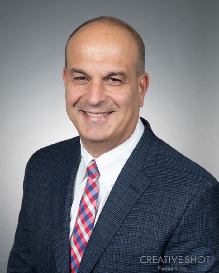 |
Steve Pateras is head of product management for the hardware analytics and test business unit within Synopsys. He has over 30 years of experience within the semiconductor industry, both on the implementation side as well as in EDA. After beginning his career at IBM, Steve joined LogicVision as one of the company’s earliest employees. He held management positions both in engineering and marketing and was VP of Marketing when the company was acquired by Mentor Graphics in 2009. At Mentor, Steve drove the company’s initial move into key vertical test markets including 3DIC and automotive. Steve joined Synopsys in 2018 and drove the creation and launch of Synopsys’ TestMAX family of test products. Most recently Steve has been driving the company’s expansion into silicon lifecycle management. Steve received his Ph.D. in Electrical Engineering from McGill University in Montreal, Canada. |
April 23, 2024
Challenges in Advanced Semiconductor Industry: Technology, Design, Testing and Talents
by Dr. Marvin Chang
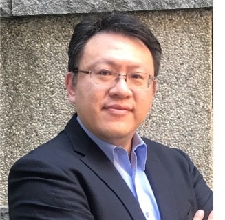 |
Dr. Chang is currently a Director of Corporate Research at TSMC and a Distinguished Professor at National Tsing Hua University (NTHU) in Taiwan. |
April 24, 2024
MEMS Design and Test Challenges
by Dr. David J. (Dave) Monk (NXP)
 |
Dr. David J. (Dave) Monk received his B.S. in ChE from the University of Iowa in 1989, his Ph.D. in ChE with the Berkeley Sensor & Actuator Center (BSAC) in 1993 from the University of California, Berkeley, and an MBA from Arizona State University |
April 24, 2024
Challenges with manufacturing test solutions for SiP/MCM requiring System Level testing with high data rate interface
by David Kim (Northrop Grumman)
Continuous advancement in fabrication and packaging technologies is pushing the boundaries of functional integration that can be achieved in a single package. Driven by the portable and wearable device market demands, RF SiP solutions have become widely popular, prompting ATE manufacturers to offer cross-domain (“RF to Bits”) test capabilities. In traditional receiver testing, high frequency RF was frequency translated to low IF signal or directly down-converted to baseband within the SiP or SoC, and then the output signals were captured using ATE analog and/or digital instrumentations for post processing. However, this test method becomes less applicable as ADC’s are reaching sampling rates in GSPS range, allowing direct RF sampling without frequency conversion. System level performance test requires digital IQ data capture via high speed SERDES bus, which comes in many different standards (e.g. – JESD204B/C, PCIe, etc.). ATE’s in today’s marketplace seem to lack proper test solutions for this application. In this keynote, we will discuss current state of test methods being evaluated to address this application along with challenges associated with high volume production testing.

| David Kim is currently a Test & Assembly Senior Manager at Advanced Technology Laboratory of Northrop Grumman Microelectronics Center. David and his RF and Digital test teams specialize in development of test solutions targeted for GaAs/SiGe RFIC’s, SI ASIC’s, SiC/SiGe/GaN Power Transistors for advanced radar sensor & EO/IR applications. Prior to joining Northrop Grumman, David served as a lead engineer and PTE manager in Broadcast division of Silicon Labs (now part of Skyworks) in Austin, TX, leading NPI and production ramp up efforts for family of Silicon Radio (Si47xx) receivers & TV (Si21xx) Tuners/Demods. David also held various engineering positions at Motorola (Fixed Products Design Center in Schaumburg, IL.) and Lucent Technologies (Wireless Division in Allentown, PA). David acquired BSEE from University of Michigan Ann Arbor, MSEE from Lehigh University, and MBA from University of Texas at Austin. |
