Monday April 28, 2025
9:00AM-10:00AM
Overview of DoD’s Microelectronics
|
|
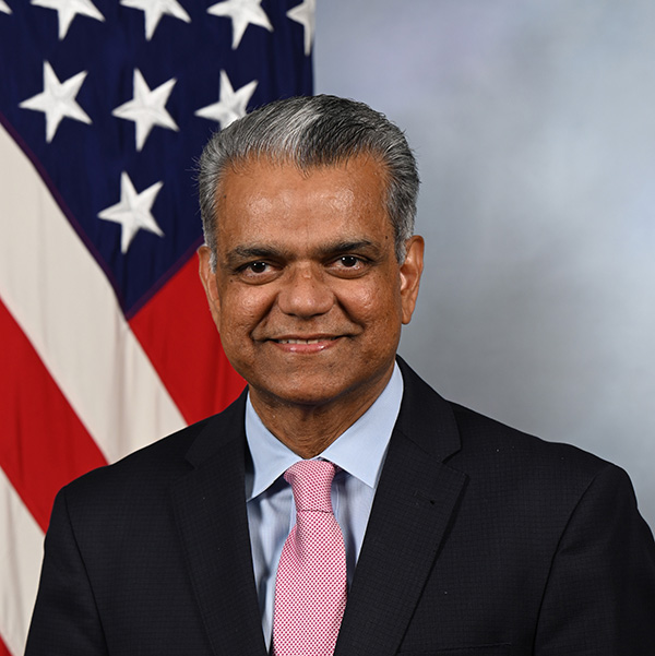
Dr. Dev ShenoyPrincipal Director for MicroelectronicsOffice of the Under Secretary of Defense for Research and EngineeringUS Department of Defense |
Biography:
Dr. Dev Shenoy joined the Office of the Under Secretary of Defense for Research and Engineering, OUSD(R&E), as the Principal Director for Microelectronics in July 2021. In this role, Dr. Shenoy is responsible for leading the Department of Defense’s research and engineering efforts in microelectronics. He has provided numerous keynote addresses, participated in multiple discussion panels, and given interviews across a broad range of industry, academic, interagency, and defense communities.
Prior to joining OUSD(R&E), Dr. Shenoy served as the Director of Microelectronics Innovation and as Director of Advanced Technologies at the University of Southern California’s Information Sciences Institute (USC/ISI).
Prior to joining USC/ISI, Dr. Shenoy served as Chief Engineer in the Advanced Manufacturing Office at the Department of Energy (DoE). In that role, he co-authored DoE’s 2015 Quadrennial Technology Review that served as a blueprint for DoE’s energy technology investments. Among other initiatives, Dr. Shenoy proposed and led a “Big Idea” for U.S. national security and economic competitiveness within the Office of Energy Efficiency and Renewable Energy on “Beyond Moore Computing” with participation from eight DoE national labs.
Prior to joining DoE, Dr. Shenoy served as a Senior Advisor at the Manufacturing and Industrial Base Policy (MIBP) Office within the Office of the Secretary of Defense (OSD) as a detailee from the Army Night Vision and Sensors Directorate at Fort Belvoir. In that role, he co-led a telecom initiative with the White House Office of Science and Technology Policy to explore U.S. opportunities in optical networks. While at OSD/MIBP, Dr. Shenoy proposed and helped develop a public-private partnership in photonics that led to the creation of the AIM Photonics Institute.
Prior to serving at OSD/MIBP, Dr. Shenoy was a program manager at the Defense Advanced Research Projects Agency where he developed and managed cutting-edge technology programs in the areas of spintronics, such as the Spin Torque Transfer Random Access Memory program, a technology that was successfully transitioned and commercialized. Dr. Shenoy also developed and led programs in photonics and micro-electromechanical systems or defense and commercial applications.
Dr. Shenoy has a Ph.D. in physics from the prestigious Indian Institute of Science in Bangalore, India, and National Science Foundation post-doctoral experience from Case Western Reserve University in Cleveland, Ohio.
Monday, April 28th, 2025
2:00-3:00PM
Catch Me If You Can: Towards Zero-ppb Defects in Analog/Mixed-signal ICs
Safety-critical applications such as biomedical and automotive depend on extremely reliable electronics that are guaranteed to function correctly over the entire application lifetime. Chasing and detecting unavoidable fabrication defects with zero escapes, not even latent ones, is key to achieving this. This keynote will highlight important steps achieved in past years to make this happen, ranging from new test metrics, proper fault models, novel design-for-test methods towards innovative test analysis methods and pioneering test generation algorithms using machine learning techniques. The second part of the keynote will provide an outlook on further techniques to make the analog/mixed-signal circuits de facto unfailing in practice.
|
|
Georges G.E. GielenProfessorKatholieke Universiteit, LeuvenBelgium |
Biography:
Georges G.E. Gielen received the MSc and PhD degrees in Electrical Engineering from the Katholieke Universiteit Leuven (KU Leuven), Belgium, in 1986 and 1990, respectively. Currently, he is Full Professor in the MICAS research division at the Department of Electrical Engineering (ESAT) at KU Leuven. From August 2013 until July 2017 he served as Vice-Rector for the Group of Sciences, Engineering and Technology. In 2018 he was visiting professor at UC Berkeley and Stanford University. From 2020 to 2024 he served as Chair of the Department of Electrical Engineering (ESAT) at KU Leuven.
His research interests are in the design of analog and mixed-signal integrated circuits, and especially in analog and mixed-signal CAD tools and design automation, including modeling, simulation, optimization and synthesis as well as testing. He is a frequently invited speaker/lecturer and coordinator/partner of several (industrial) research projects in this area, including an ERC Advanced Grant. He has (co-)authored 10 books and more than 700 publications in edited books, international journals and conference proceedings. He is a 1997 Laureate of the Belgian Royal Academy of Sciences, Literature and Arts in the discipline of Engineering. He is Fellow of the IEEE since 2002, and received the IEEE CAS Mac Van Valkenburg award in 2015 and the IEEE CAS Charles Desoer award in 2020, as well as the EDAA Achievement Award in 2021. He is an elected member of the Royal Flemish Academy of Belgium in the class of Technical Sciences, and of the Academia Europaea.
Tuesday, April 29, 2025
8:30AM-9:30AM
Challenges in Testing and Reliability of BioChips
The increasing miniaturization and integration of microelectronics enables new highly integrated, multiphysics microsystems that place instrumentation in intimate contact with sensing and actuation capabilities. These lab-on-CMOS (LoCMOS) systems are an extension of lab-on-a-chip (LOC) systems, miniaturized devices that integrate several laboratory functions onto a single “chip”. LoCMOS systems tie sensing closely to signal processing, detection, and actuation, leading to overall systems with significantly smaller size and also the potential for completely novel measurements that cannot be performed using traditional approaches. This tight low-level integration of active electronics with sensing poses a number of distinct challenges in testing and reliability in these systems. This talk will provide an overview of LoCMOS systems and technology and their distinct challenges in testing and reliability for diverse LoCMOS applications, including state of the art and future directions in packaging, optical inspection, ground truth validation, and calibration. By establishing dense and information-rich interfaces, LoCMOS systems offer the potential for disruptive changes in biosensing and medical diagnostics in the near future.
|
|
Pamela AbshireProfessorFischell Institute FellowUniversity of Maryland, College Park |
Biography:
Pamela Abshire is Professor of Electrical and Computer Engineering and the Institute for Systems Research at the University of Maryland, College Park. She received the BS in Physics from the California Institute of Technology in 1992, and the MS and PhD in Electrical and Computer Engineering from Johns Hopkins University in 1997 and 2002. In between CalTech and JHU, she worked for the biomedical device company Medtronic. She is internationally known for her work in low power mixed-signal integrated circuits (IC), adaptive ICs and IC sensors, and CMOS biosensors. Her research focuses on better understanding and exploiting the tradeoffs between performance and resources in natural and engineered systems, including hybrid devices incorporating CMOS, MEMS, optoelectronics, microfluidics, and biological components. Her honors include an NSF CAREER award (2003), elevation to IEEE Fellow (2018) for contributions to CMOS biosensors, and recognition as a Distinguished Scholar- Teacher at the University of Maryland (2021). She has authored 150+ publications and 3 patents. She served on the Emerging Technologies and Research Advisory Committee for the U.S. Department of Commerce (2008-2018), on the Board of Governors for the IEEE Circuits and Systems Society (2013-2018 & 2024-2026), the IEEE Fellow Committee (2019-2021 & 2025-2026), as General Co-Chair for the 2017 IEEE International Symposium on Circuits and Systems, on the Microsystems Exploratory Council for the DARPA Microsystem Technology Office, and as General Co-Chair for the 2023 IEEE International Midwest Symposium on Circuits and Systems.
Wednesday, April 30, 2025
8:30AM-9:30AM
|
|
Eric MakaraMicroelectronics Commons 5G/6G LeadNaval Research Laboratory |
Biography:
Eric Makara is the Section Head of the Systems Integration & Instrumentation Section, within the Networks and Communication Systems Branch, of the U.S. Naval Research Laboratory (NRL) in Washington, DC. In his position, Mr. Makara leads a team of researchers specializing in wireless communications systems and networks. He has led and contributed to projects in spectrum sharing, dynamic spectrum management, software defined radio, waveforms for air combat training, tactical wireless communications, 5G technologies, multifunction communications systems integration, and wireless network modeling and emulation.
Mr. Makara is the 5G/6G Technical Execution Area Lead for the DoD Microelectronics Commons program, supporting the Office of the Under Secretary of Defense for Research & Engineering (OUSD(R&E)). In this role, Mr. Makara is responsible for technical oversight, management, and strategy of the 5G/6G technologies portfolio. The Microelectronics Commons is a national network of prototyping innovation hubs that are creating direct pathways to commercialization for US microelectronics from “lab to fab”. Microelectronics Commons supports six critical technology areas, including 5G/6G technologies, Artificial Intelligence (AI) Hardware, Commercial Leap-Ahead technologies, Electromagnetic Warfare (EW), Secure Edge / Internet of Things (IoT) Computing, and Quantum.
Wednesday, April 30, 2025
2:30PM-3:30PM
Chiplet Architectures, Advanced Packaging, and the Importance of Test
AMD is an industry leader in the use of chiplet architectures and advanced and packaging to enhance its products. Over the past decade, this has included volume production of 2.5D technologies including silicon interposer, organic RDL interposer, and embedded fan-out bridge (EFB), as well as hybrid bond 3D logic-on-SRAM stacking, and cost-effective chiplet re-use with multi-chip modules. The recently released AMD Instinct™ MI300 AI chip combines many of these technologies into ‘3.5D’ packaging – 3D hybrid bond logic die stacks are connected together and to eight total HBM DRAM stacks using a 2.5D silicon interposer, resulting in a module with massive compute capacity and the near memory capacity and bandwidth needed to support it. This talk will examine the role of chiplet architecture and advanced packaging in current product offerings, and discuss the scaling trends that will drive new advanced packaging technologies in the future, largely driven by the AI accelerator market. Throughout, connections will be made to the importance of Design Technology Co-Optimization (DTCO) between SoC design, packaging technology, silicon technology, and sort/test.
 |
Dr. Bill LambertFellowAMD |
Biography:
William Lambert is a Fellow of AMD, Inc. where he leads a team defining the packaging solutions for next-generation products including datacenter GPUs and CPUs, client GPUs and CPUs, and more. Prior to joining AMD, he was a Senior Principal Engineer in the Assembly & Test Technology Development group at Intel Corporation, where he held leadership roles in packaging architecture definition, power delivery and integrated voltage regulation technology development, and RF packaging development. He received his Ph.D. in electrical engineering from Arizona State University with a focus on low-voltage DC-DC power electronics for computer systems, and his M.S. and B.S. degrees from Rochester Institute of Technology.


